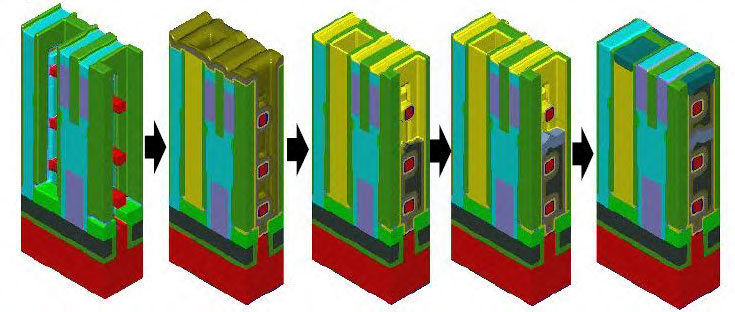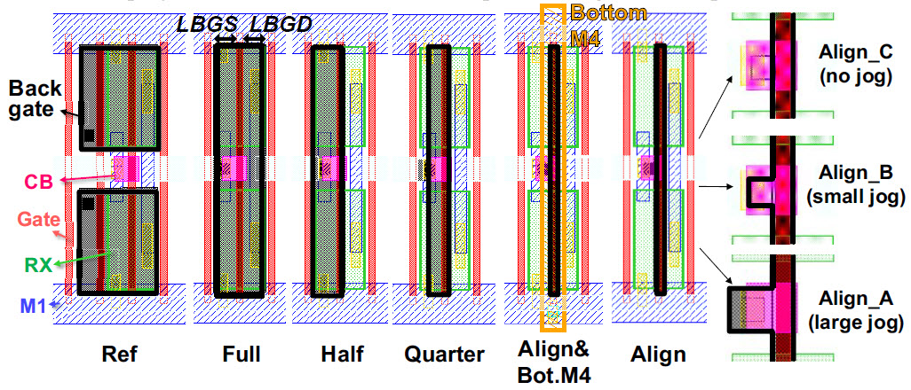
Design Technology Co-Optimization of 3D-monolithic standard cells and SRAM exploiting dynamic back-bias for ultra-low-voltage operation
December 29, 2017
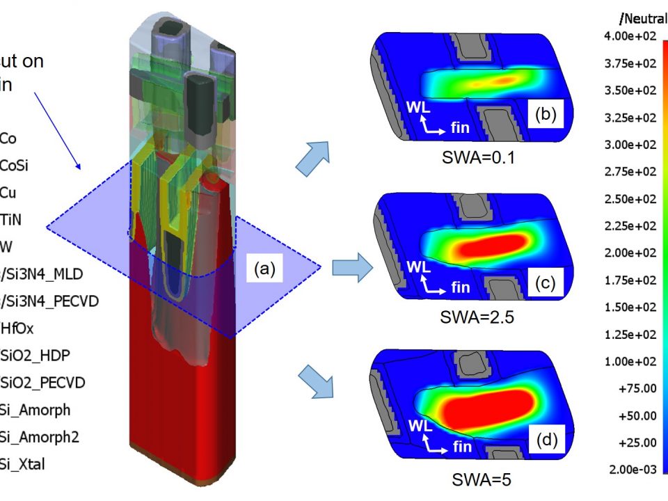
Understanding the Effect of Variability in Bulk FinFET Device Performance
April 27, 2018You must have an account on our Customer Portal to access this content. If you already have an account, please log in using the form below or to the right. If you do not have an account, we invite you to request an account.
Whitepaper: Self-Aligned Block and Fully Self-Aligned Via for iN5 Metal 2 Self-Aligned Quadruple Patterning

To download your free white paper, please fill out the form below:
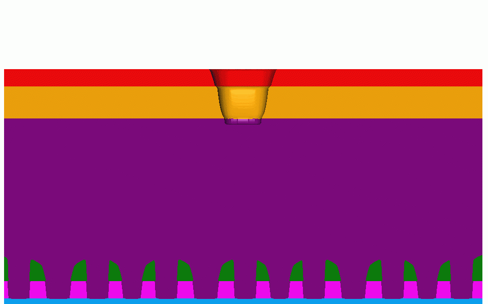
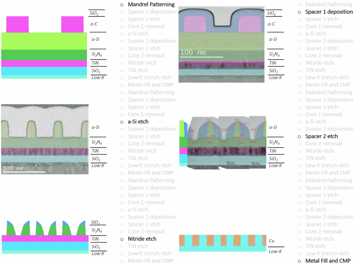
This paper assesses Self-Aligned Block (SAB) and Fully Self-Aligned Via (FSAV) approaches to patterning using a iN5 (imec node 5 nm) vehicle and Metal 2 Self-Aligned Quadruple Patterning. We analyze SAB printability in the lithography process using process optimization, and demonstrate the effect of SAB on patterning yield for a (8 M2 lines x 6 M1 lines x 6 Via) structure. We show that FSAV, compared to standard Via patterning, has no beneficial impact but prevents dielectric breakdown between two adjacent M1 lines.
Benjamin Vincent, Joern-Holger Franke, Aurelie Juncker, Frederic Lazzarino, Gayle Murdoch, Sandip Halder, Joseph Ervin
https://doi.org/10.1117/12.2298761
© 2018 Society of Photo Optical Instrumentation Engineers (SPIE). One print or electronic copy may be made for personal use only. Systematic reproduction and distribution, duplication of any material in this publication for a fee or for commercial purposes, or modification of the contents of the publication are prohibited.
You might also be interested in:
- You must have an account on our Customer Portal to access this content. If you already have an account, please log in using the form below or to the right. […]
- You must have an account on our Customer Portal to access this content. If you already have an account, please log in using the form below or to the right. […]
- You must have an account on our Customer Portal to access this content. If you already have an account, please log in using the form below or to the right. […]
- You must have an account on our Customer Portal to access this content. If you already have an account, please log in using the form below or to the right. […]
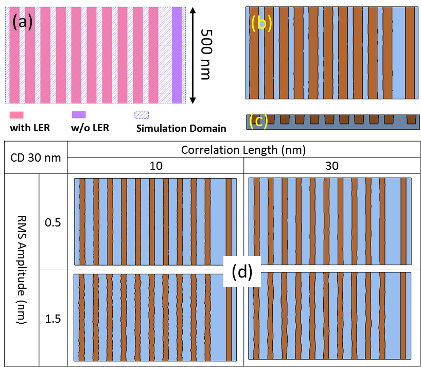
Impact of EUV Resist Thickness on Local Critical Dimension Uniformities for <30 nm CD Via Patterning
Impact of EUV Resist Thickness on Local Critical Dimension Uniformities for <30 nm CD Via Patterning
You must have an account on our Customer Portal to access this content. If you already have an account, please log in using the form below or to the right. […]- You must have an account on our Customer Portal to access this content. If you already have an account, please log in using the form below or to the right. […]
- You must have an account on our Customer Portal to access this content. If you already have an account, please log in using the form below or to the right. […]
- You must have an account on our Customer Portal to access this content. If you already have an account, please log in using the form below or to the right. […]
- You must have an account on our Customer Portal to access this content. If you already have an account, please log in using the form below or to the right. […]
- You must have an account on our Customer Portal to access this content. If you already have an account, please log in using the form below or to the right. […]


