Optimizing DRAM Development using Directed Self-Assembly (DSA)
February 13, 2017
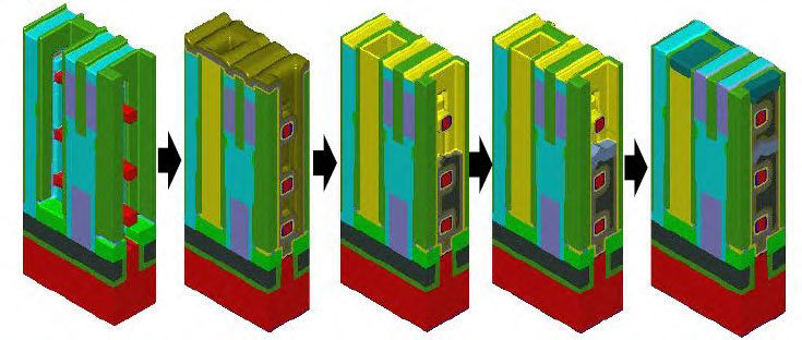
Modeling of Tone Inversion Process Flow for N5 Interconnect to Characterize Block Tip to Tip
September 21, 2017You must have an account on our Customer Portal to access this content. If you already have an account, please log in using the form below or to the right. If you do not have an account, we invite you to request an account.
Whitepaper: Understanding how small variations in photoresist shape significantly impact multi-patterning yield

To download your free white paper, please fill out the form below:
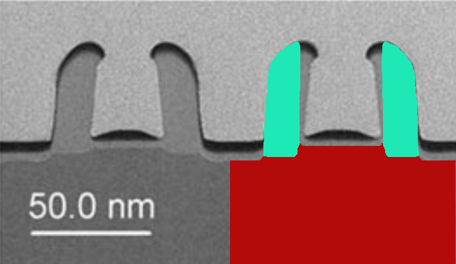
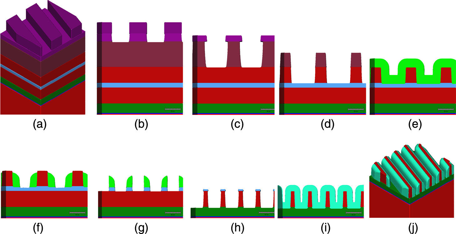
Multi-patterning schemes such as Self-Aligned Double Patterning (SADP) and Self-Aligned Quadruple Patterning (SAQP) have been used to successfully increase semiconductor device density, circumventing prior physical limits in pattern density. However, the number of processing steps needed in these patterning schemes can make it difficult to directly translate a lithographic mask pattern to a final product. Unfortunately, it is not straightforward to understand how a given photoresist shape will affect finished patterns on a chip. Small changes in the photoresist shape can unexpectedly modify the final pattern on chip, due to the complexity of subsequent process steps following photolithography.
Virtual fabrication is a computerized technique to perform predictive, three dimensional modeling of semiconductor fabrication processes. Virtual fabrication allows engineers to test semiconductor process changes and process variability in minutes or hours, instead of the weeks or months required to test their designs using actual semiconductor wafers. SEMulator3D® is a virtual fabrication solution that can model process variability under complex patterning schemes and process flows.
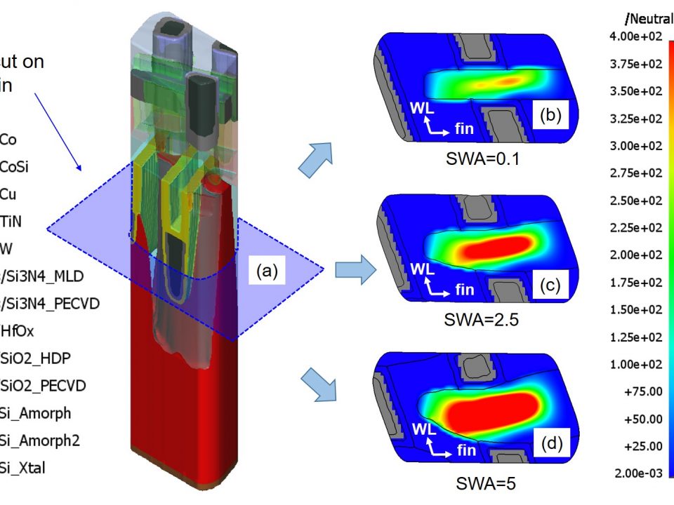
SEMulator3D can be used to model the impact of variability in photoresist shape on the final patterns produced in a semiconductor device. In this study, we used SEMulator3D to model how photoresist shape affects the fin shape and back-end-of-line (BEOL) capacitance in a FinFET device. Variations in final patterns obtained using a self-aligned multi-patterning scheme were predicted, under conditions of sidewall profile variability in the starting photoresist shape.
Mustafa B. Akbulut ; Jiangjiang Gu ; Andras Pap ; Vasanth Allampalli ; Daniel Faken ; Joseph Ervin ; Ken Greiner ; David Fried, “Investigation of 3D photoresist profile effect in self-aligned patterning through virtual fabrication”, Proc. SPIE 10147, Optical Microlithography XXX, 101470G (March 24, 2017);
http://dx.doi.org/10.1117/12.2258157 Copyright 2017 Society of Photo Optical Instrumentation Engineers. One print or electronic copy may be made for personal use only. Systematic reproduction and distribution, duplication of any material in this paper for a fee or for commercial purposes, or modification of the content of the paper are prohibited.
You might also be interested in:
- You must have an account on our Customer Portal to access this content. If you already have an account, please log in using the form below or to the right. […]
- You must have an account on our Customer Portal to access this content. If you already have an account, please log in using the form below or to the right. […]
- You must have an account on our Customer Portal to access this content. If you already have an account, please log in using the form below or to the right. […]
- You must have an account on our Customer Portal to access this content. If you already have an account, please log in using the form below or to the right. […]
- You must have an account on our Customer Portal to access this content. If you already have an account, please log in using the form below or to the right. […]
- You must have an account on our Customer Portal to access this content. If you already have an account, please log in using the form below or to the right. […]
- You must have an account on our Customer Portal to access this content. If you already have an account, please log in using the form below or to the right. […]
- You must have an account on our Customer Portal to access this content. If you already have an account, please log in using the form below or to the right. […]
- You must have an account on our Customer Portal to access this content. If you already have an account, please log in using the form below or to the right. […]
- You must have an account on our Customer Portal to access this content. If you already have an account, please log in using the form below or to the right. […]
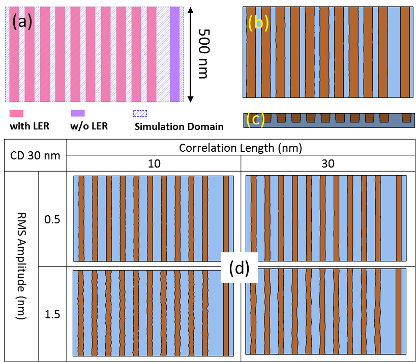
Impact of EUV Resist Thickness on Local Critical Dimension Uniformities for <30 nm CD Via Patterning
Impact of EUV Resist Thickness on Local Critical Dimension Uniformities for <30 nm CD Via Patterning
You must have an account on our Customer Portal to access this content. If you already have an account, please log in using the form below or to the right. […]- You must have an account on our Customer Portal to access this content. If you already have an account, please log in using the form below or to the right. […]


