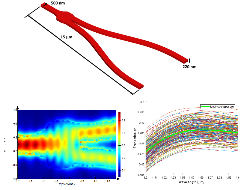
Effects of a Random Process Variation on the Transfer Characteristics of a Fundamental Photonic Integrated Circuit Component
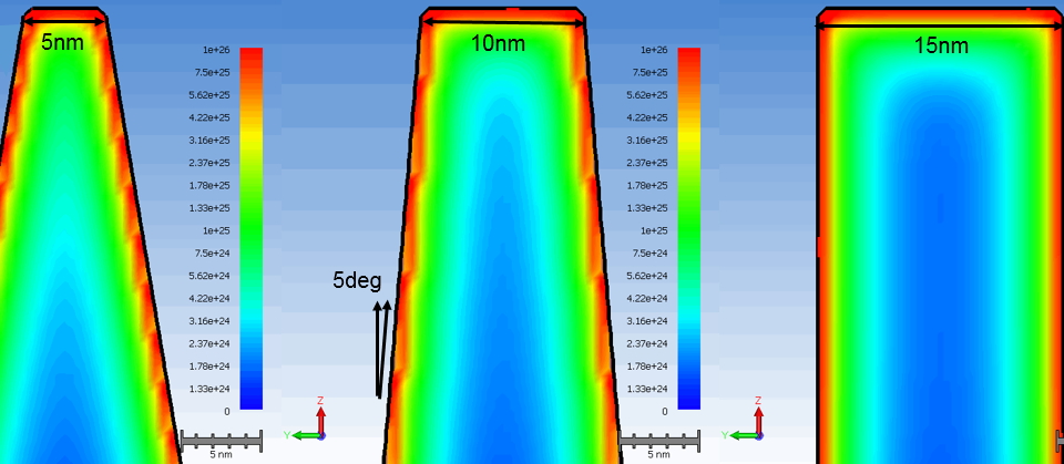
September 14, 2018Process Modeling Exploration for 8 nm Half-Pitch Interconnects
February 1, 2019You must have an account on our Customer Portal to access this content. If you already have an account, please log in using the form below or to the right. If you do not have an account, we invite you to request an account.
Whitepaper: Innovative Solutions to Increase 3D NAND Flash Memory Density

To download your free white paper, please fill out the form below:
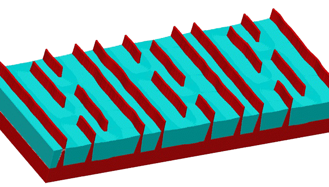
In the last 10 years, 3D NAND flash memory has enabled a new generation of non-volatile solid-state storage useful in nearly every electronic device imaginable. 3D NAND can achieve data densities exceeding those of 2D NAND structures, due to the relative ease of 3D integration, even when fabricated on later generation technology nodes. 3D NAND structures contain vertical channels which orthogonally pierce an alternating stacked conductor/insulator structure. Word lines are individually accessed through a staircase-like structure. This whitepaper will discuss the operating principles and manufacturing process challenges of 3D NAND structures, along with techniques to advance the data density of 3D NAND devices.
You might also be interested in:
- You must have an account on our Customer Portal to access this content. If you already have an account, please log in using the form below or to the right. […]
- You must have an account on our Customer Portal to access this content. If you already have an account, please log in using the form below or to the right. […]
- You must have an account on our Customer Portal to access this content. If you already have an account, please log in using the form below or to the right. […]
- You must have an account on our Customer Portal to access this content. If you already have an account, please log in using the form below or to the right. […]
- You must have an account on our Customer Portal to access this content. If you already have an account, please log in using the form below or to the right. […]
Impact of EUV Resist Thickness on Local Critical Dimension Uniformities for <30 nm CD Via Patterning
Impact of EUV Resist Thickness on Local Critical Dimension Uniformities for <30 nm CD Via Patterning
You must have an account on our Customer Portal to access this content. If you already have an account, please log in using the form below or to the right. […]- You must have an account on our Customer Portal to access this content. If you already have an account, please log in using the form below or to the right. […]
- You must have an account on our Customer Portal to access this content. If you already have an account, please log in using the form below or to the right. […]
- You must have an account on our Customer Portal to access this content. If you already have an account, please log in using the form below or to the right. […]
- You must have an account on our Customer Portal to access this content. If you already have an account, please log in using the form below or to the right. […]
- You must have an account on our Customer Portal to access this content. If you already have an account, please log in using the form below or to the right. […]

